PIC18F2480/2580/4480/4580
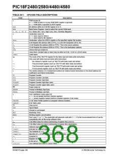
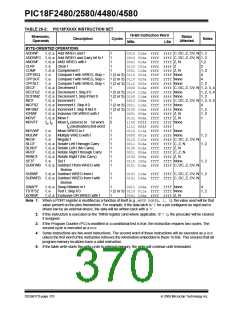
TABLE 26-2: PIC18FXXXX INSTRUCTION SET
16-Bit Instruction Word
MSb LSb
Mnemonic,
Operands
Status
Affected
Description
Cycles
Notes
BYTE-ORIENTED OPERATIONS
ADDWF f, d, a Add WREG and f
ADDWFC f, d, a Add WREG and Carry bit to f
1
0010 01da ffff ffff C, DC, Z, OV, N 1, 2
0010 00da ffff ffff C, DC, Z, OV, N 1, 2
1
1
1
1
ANDWF
CLRF
COMF
f, d, a AND WREG with f
f, a Clear f
f, d, a Complement f
0001 01da ffff ffff Z, N
0110 101a ffff ffff Z
0001 11da ffff ffff Z, N
1,2
2
1, 2
4
CPFSEQ
CPFSGT
CPFSLT
DECF
DECFSZ
DCFSNZ
INCF
f, a
f, a
f, a
Compare f with WREG, Skip = 1 (2 or 3) 0110 001a ffff ffff None
Compare f with WREG, Skip > 1 (2 or 3) 0110 010a ffff ffff None
Compare f with WREG, Skip < 1 (2 or 3) 0110 000a ffff ffff None
4
1, 2
f, d, a Decrement f
f, d, a Decrement f, Skip if 0
f, d, a Decrement f, Skip if Not 0
f, d, a Increment f
1
0000 01da ffff ffff C, DC, Z, OV, N 1, 2, 3, 4
1 (2 or 3) 0010 11da ffff ffff None
1 (2 or 3) 0100 11da ffff ffff None
1
1, 2, 3, 4
1, 2
0010 10da ffff ffff C, DC, Z, OV, N 1, 2, 3, 4
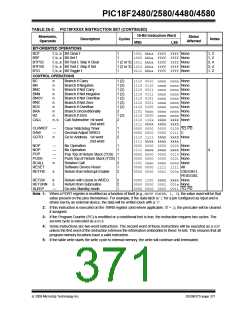
INCFSZ
INFSNZ
IORWF
MOVF
f, d, a Increment f, Skip if 0
f, d, a Increment f, Skip if Not 0
f, d, a Inclusive OR WREG with f
f, d, a Move f
fs, fd Move fs (source) to 1st word
fd (destination)2nd word
1 (2 or 3) 0011 11da ffff ffff None
1 (2 or 3) 0100 10da ffff ffff None
4
1, 2
1, 2
1
1
1
2
0001 00da ffff ffff Z, N
0101 00da ffff ffff Z, N
1100 ffff ffff ffff None
1111 ffff ffff ffff
MOVFF
MOVWF
MULWF
NEGF
RLCF
RLNCF
RRCF
f, a
f, a
f, a
Move WREG to f
Multiply WREG with f
Negate f
1
1
1
1
1
1
1
1
1
0110 111a ffff ffff None
0000 001a ffff ffff None
0110 110a ffff ffff C, DC, Z, OV, N
0011 01da ffff ffff C, Z, N
0100 01da ffff ffff Z, N
0011 00da ffff ffff C, Z, N
0100 00da ffff ffff Z, N
0110 100a ffff ffff None
0101 01da ffff ffff C, DC, Z, OV, N
1, 2
1, 2
f, d, a Rotate Left f through Carry
f, d, a Rotate Left f (No Carry)
f, d, a Rotate Right f through Carry
f, d, a Rotate Right f (No Carry)
RRNCF
SETF
f, a
Set f
1, 2
SUBFWB f, d, a Subtract f from WREG with
Borrow
SUBWF
f, d, a Subtract WREG from f
1
1
0101 11da ffff ffff C, DC, Z, OV, N 1, 2
0101 10da ffff ffff C, DC, Z, OV, N
SUBWFB f, d, a Subtract WREG from f with
Borrow
SWAPF
TSTFSZ
XORWF
f, d, a Swap Nibbles in f
f, a Test f, Skip if 0
f, d, a Exclusive OR WREG with f
1
0011 10da ffff ffff None
4
1, 2
1 (2 or 3) 0110 011a ffff ffff None
0001 10da ffff ffff Z, N
1
Note 1: When a PORT register is modified as a function of itself (e.g., MOVF PORTB, 1, 0), the value used will be that
value present on the pins themselves. For example, if the data latch is ‘1’ for a pin configured as input and is
driven low by an external device, the data will be written back with a ‘0’.
2: If this instruction is executed on the TMR0 register (and where applicable, ‘d’ = 1), the prescaler will be cleared
if assigned.
3: If the Program Counter (PC) is modified or a conditional test is true, the instruction requires two cycles. The
second cycle is executed as a NOP.
4: Some instructions are two-word instructions. The second word of these instructions will be executed as a NOP
unless the first word of the instruction retrieves the information embedded in these 16 bits. This ensures that all
program memory locations have a valid instruction.
5: If the table write starts the write cycle to internal memory, the write will continue until terminated.
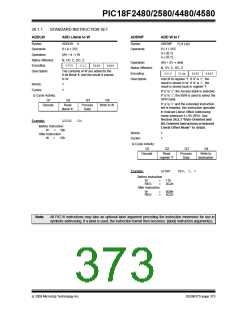
DS39637D-page 370
© 2009 Microchip Technology Inc.

 MICROCHIP [ MICROCHIP ]