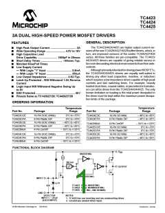
3A DUAL HIGH-SPEED POWER MOSFET DRIVERS
TC4423
TC4424
TC4425
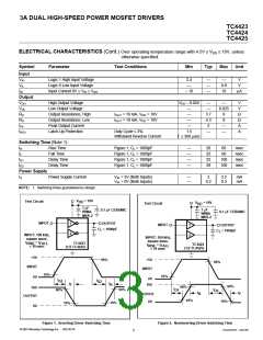
ELECTRICAL CHARACTERISTICS (Cont.) Over operating temperature range with 4.5V ≤ VDD ≤ 18V, unless
otherwise specified.
Symbol
Parameter
Test Conditions
Min
Typ
Max
Unit
Input
VIH
Logic 1 High Input Voltage
Logic 0 Low Input Voltage
Input Current 0V ≤ VIN ≤ VDD
2.4
—
—
—
—
—
0.8
10
V
V
VIL
IIN
– 10
µA
Output
VOH
VOL
RO
High Output Voltage
Low Output Voltage
Output Resistance, High
Output Resistance, Low
Peak Output Current
Latch-Up Protection
VDD – 0.025
—
—
3.7
4.3
3
—
0.025
8
V
V
Ω
Ω
A
A
—
—
—
—
IOUT = 10 mA, VDD = 18V
IOUT = 10 mA, VDD = 18V
RO
8
IPK
—
IREV
Duty Cycle ≤ 2%
1.5
—
—
Withstand Reverse Current
t ≤ 300 µsec
Switching Time (Note 1)
tR
Rise Time
Fall Time
Figure 1, CL = 1800pF
Figure 1, CL = 1800pF
Figure 1, CL = 1800pF
Figure 1, CL = 1800pF
—
—
—
—
28
32
32
38
60
60
nsec
nsec
nsec
nsec
tF
tD1
Delay Time
Delay Time
100
100
tD2
Power Supply
IS
Power Supply Current
VIN = 3V (Both Inputs)
VIN = 0V (Both Inputs)
—
—
2
0.2
3.5
0.3
mA
mA
NOTE: 1. Switching times guaranteed by design.
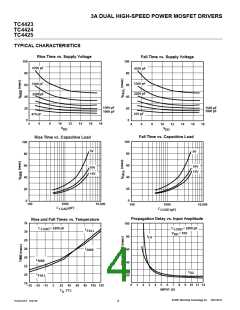
V
= 16V
Test Circuit
DD
V
= 16V
Test Circuit
DD
1 µF
WIMA
MKS-2
1 µF
WIMA
MKS-2
0.1 µF CERAMIC
0.1 µF CERAMIC
INPUT
1
2
OUTPUT
INPUT
1
2
OUTPUT
C
= 1800pF
L
C
= 1800pF
L
INPUT: 100 kHz,
square wave,
INPUT: 100 kHz,
square wave,
t
= t
TC4423
(1/2 TC4425)
RISE FALL
TC4424
(1/2 TC4425)
t
= t
RISE FALL
≤ 10 nsec
≤ 10 nsec
+5V
+5V
90%
90%
INPUT
INPUT
10%
10%
0V
0V
t
t
D1
D2
t
t
F
R
16V
90%
10%
90%
16V
t
90%
t
D2
90%
D1
t
t
F
R
OUTPUT
0V
OUTPUT
0V
10%
10%
10%
Figure 1. Inverting Driver Switching Time
Figure 2. Noninverting Driver Switching Time
© 2001 Microchip Technology Inc. DS21421A
TC4423/4/5-6 10/21/96
3

 MICROCHIP [ MICROCHIP ]