Freescale Semiconductor, Inc.
Appendix: CGM Practical Aspects
A Few Hints For The CGM Crystal Oscillator Application
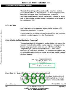
quiescent point is reached. Controlling this final peak to peak amplitude
can be performed by three means:
1. Reducing the values of C1 and C2. This decreases the loading so
that the necessary gm value required to sustain oscillation can be
smaller. The consequently smaller current will be reached with a
larger ‘extal’ swing.
2. Using VDDPLL=VSS (i.e. shutting off the PLL). Doing so
increases the starting current by approximately 50%. All other
parameters staying the same, a larger ‘extal’ swing will be required
to reduce this starting current to its quiescent value.
3. Also, placing a high value resistor (>1MΩ) across the EXTAL and
XTAL pins significantly increased the oscillation amplitude.
Because this complicates the design analysis as it transforms a
pure susceptance jωC1 into a complex admittance G+jωC1,
Motorola cannot promote this application trick.
21.3.5 What Do I Do In Case The Oscillator Does Not Start-up?
1. First, verify that the application schematic respects the principle of
operation, i.e. crystal mounted between EXTAL and VSS,
Capacitor C1 between XTAL and EXTAL, Capacitor C2 between
XTAL and VSS, nothing else. This is not the conventional MCU
application schematic of the Pierce oscillator as it can be seen on
other HC12 derivatives!
2. Re-consider the choice of the tuning capacitors.
3. The oscillator circuitry is powered internally from a core VDD pad
and the return path is the VSSPLL pad. Verify on the application
PCB the correct connection of these pads (especially VSSPLL),
but also verify the waveform of the VDD voltage as it is imposed
on the pad. Sometimes external components (for instance choke
inductors), can cause oscillations on the power line. This is of
course detrimental to the oscillator circuitry.
4. If possible, consider using a resonator with built-in tuning
capacitors. They may offer better performances with respect to
their discrete elements implementation.
68HC(9)12D60 — Rev 4.0
MOTOROLA
Advance Information
Appendix: CGM Practical Aspects
389
For More Information On This Product,
Go to: www.freescale.com

 MOTOROLA [ MOTOROLA ]