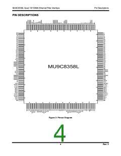
3LQꢄ'HVꢈULSWLRQV
08ꢀ&ꢁꢂꢃꢁ/ꢄ4XDGꢄꢅꢆꢇꢅꢆꢆ0Eꢄ(WKHUQHWꢄ)LOWHUꢄ,QWHUIDꢈH
6LJQDOꢀ&KDUDꢂWHULVWLꢂV
All signals are implemented in CMOS technology with TTL levels. Signal names that start with a slash (“/”) are active
LOW. Inputs should never be left floating. Pins designated as "Reserved" must not be connected to any external circuitry.
Refer to the Electrical Characteristics section for more information.
0,,ꢀ,QWHUIDꢂHVꢀ>3RUWVꢀ$ꢀWKURXJKꢀ'?
7DJꢀ3RUWꢀ,QWHUIDꢂHVꢀ>3RUWVꢀ$ꢀWKURXJKꢀ'?
5;'ꢐꢊꢑꢆ@B>$±'?ꢀ>5HꢂHLYHꢀ'DWDꢁꢀ,QSXWꢁꢀ77/?
5(-B>$±'?ꢀ>5HMHꢂWꢁꢀ2XWSXWꢁꢀ77/?
RXD[3:0] is the 4-bit MII Receive Data nibble (see
Timing Diagrams: Timing Data for RXD, RX_DV, and
RX_ER).
REJ is the reject packet command issued by the
MU9C8358L; the minimum length is 110 nanoseconds.
REJ is driven HIGH to reject a data frame, and can be
detected by and responded to by the MAC devices from 2
bit times after SFD to 512 bit times (64 byte times) after
SFD. The REJ signal can be made active LOW by setting
Bit 0 in the SSCFG register. (See Timing Diagrams:
Timing Data for REJ (Base 100.))
5;B'9B>$±'?ꢀ>5HꢂHLYHꢀ'DWDꢀ9DOLGꢁꢀ,QSXWꢁꢀ77/?
Data Valid is on RX_DV; RX_DV is asserted by the PHY
at the beginning of the first nibble of the data frame and
deasserted at the end of the last nibble of the frame. It
indicates that the data is synchronous to RX_CLK and is
itself synchronous to the clock (see Timing Diagrams:
Timing Data for RXD, RX_DV, and RX_ER).
)5;B(5B>$±'?ꢀ>)UDPHꢀ(UURUꢁꢀ2XWSXWꢁꢀ77/?
The Forced Receive Error pins provide the logical OR of
the RX_ER and REJ lines for the appropriate MII port (see
Timing Diagrams: Timing Data for FRX_ER in Relation
to REJ and RX_ER).
5;B(5B>$±'?ꢀ>5HꢂHLYHꢀ(UURUꢁꢀ,QSXWꢁꢀ77/?
RX_ER indicates a data symbol error in 100Mb/s mode or
any other error that the PHY can detect, even if the MAC
is not capable of detecting that error (see Timing
Diagrams: Timing Data for RXD, RX_DV, and RX_ER).
73B6'B>$±'?ꢀ>7DJꢀ3RUWꢀ'DWDꢁꢀ2XWSXWꢁꢀ77/?
The Tag Port Serial Data pin carries the destination Port
ID to external circuitry as soon as it is collected from the
CAM (see Timing Diagrams: Timing Data for Tag Ports
TP_DV and TP_SD).
5;B&/.B>$±'?ꢀ>5HꢂHLYHꢀ&ORꢂNꢁꢀ,QSXWꢁꢀ77/?
RX_CLK is the receive clock recovered from the data by
the PHY. It is equal to 25 MHz in 100Base-X mode or 2.5
MHz in 10Base-X mode.
73B'9B>$±'?ꢀ>7DJꢀ3RUWꢀ'DWDꢀ9DOLGꢁꢀ2XWSXWꢁꢀ77/?
&56B>$±'?ꢀ>&DUULHUꢀ6HQVHꢁꢀ,QSXWꢁꢀ77/?
The Tag Port Data Valid pins are driven HIGH for as long
as unread data exists for each Destination Port ID. Pins
TP_SD_A through TP_SD_D carry the Destination Port
ID (4 bits) to external circuitry as soon as it is collected
from the CAM (see Timing Diagrams: Timing Data for
Tag Ports TP_DV and TP_SD).
Carrier sense CRS indicates that the medium is active
(non-idle) and remains asserted during a collision. For Rx
or Tx: CRS is HIGH in 10/100Base-X half-duplex mode;
for Rx it is HIGH in repeater, full-duplex, and loopback
modes. CRS is not synchronized to RX_CLK.
&2/B>$±'?ꢀ>&ROOLVLRQꢁꢀ,QSXWꢁꢀ77/?
Collision detect COL is asserted by the PHY upon
detection of a collision on the medium and remains
asserted as long as the collision persists. It is HIGH in
half-duplex modes and remains HIGH for 1 microsecond
following the end of transmission; it is LOW in
full-duplex mode. It is asserted in response to
signal_quality_error message from the PMA in 10Base-X
Heartbeat mode.
5HYꢇꢀꢄ
ꢋ

 MUSIC [ MUSIC SEMICONDUCTORS ]