NCP1200
If the leakage inductance is kept low, the MTD1N60E can
withstand accidental avalanche energy, e.g. during a
high−voltage spike superimposed over the mains, without
the help of a clamping network. If this leakage path
permanently forces a drain−source voltage above the
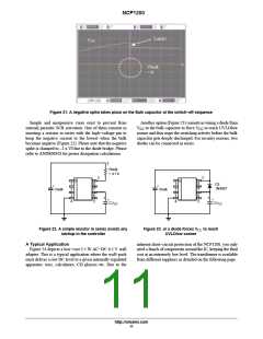
MOSFET BVdss (600 V), a clamping network is mandatory
and must be built around Rclamp and Clamp. Dclamp shall
react extremely fast and can be a MUR160 type. To calculate
the component values, the following formulas will help you:
V
: the clamping ripple, could be around 20 V
Another option lies in implementing a snubber network
ripple
which will damp the leakage oscillations but also provide
more capacitance at the MOSFET’s turn−off. The peak
voltage at which the leakage forces the drain is calculated
by:
L
leak
V
+ Ip @
Ǹ
max
C
lump
R
clamp =
where C
represents the total parasitic capacitance seen
lump
at the MOSFET opening. Typical values for Rsnubber and
Csnubber in this 4W application could respectively be 1.5
kW and 47 pF. Further tweaking is nevertheless necessary to
tune the dissipated power versus standby power.
2 @ V
@ (V
* (V
) Vf sec) @ N)
out
clamp
clamp
L
@ Ip2 @ Fsw
leak
V
clamp
@ Fsw @ R
C
+
Available Documents
clamp
V
ripple
clamp
“Implementing the NCP1200 in Low−cost AC−DC
Converters”, AND8023/D.
with:
V
: the desired clamping level, must be selected to be
clamp
“Conducted EMI Filter Design for the NCP1200’’,
AND8032/D.
between 40 V to 80 V above the reflected output voltage
when the supply is heavily loaded.
“Ramp Compensation for the NCP1200’’, AND8029/D.
V
+ Vf: the regulated output voltage level + the secondary
out
TRANSient and AC models available to download at:
http://onsemi.com/pub/NCP1200
diode voltage drop
L
leak
: the primary leakage inductance
NCP1200 design spreadsheet available to download at:
http://onsemi.com/pub/NCP1200
N: the Ns:Np conversion ratio
: the switching frequency
F
SW
ORDERING INFORMATION
Device
†
Type
Marking
Package
Shipping
NCP1200P40
1200P40
PDIP−8
50 Units / Rail
NCP1200P40G
1200P40
PDIP−8
50 Units / Rail
(Pb−Free)
F
SW
= 40 kHz
NCP1200D40R2
200D4
200D4
SOIC−8
2500 Units /Reel
2500 Units /Reel
NCP1200D40R2G
SOIC−8
(Pb−Free)
NCP1200P60
1200P60
1200P60
PDIP−8
50 Units / Rail
50 Units / Rail
NCP1200P60G
PDIP−8
(Pb−Free)
F
SW
= 60 kHz
NCP1200D60R2
200D6
200D6
SOIC−8
2500 Units /Reel
2500 Units /Reel
NCP1200D60R2G
SOIC−8
(Pb−Free)
NCP1200P100
1200P100
1200P100
PDIP−8
50 Units / Rail
50 Units / Rail
NCP1200P100G
PDIP−8
(Pb−Free)
F
SW
= 100 kHz
NCP1200D100R2
NCP1200D100R2G
200D1
200D1
SOIC−8
2500 Units / Reel
2500 Units / Reel
SOIC−8
(Pb−Free)
†For information on tape and reel specifications, including part orientation and tape sizes, please refer to our Tape and Reel Packaging
Specifications Brochure, BRD8011/D.
http://onsemi.com
14

 ONSEMI [ ONSEMI ]