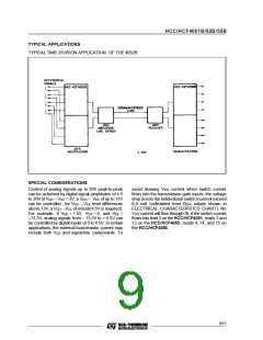
HCC/HCF4051B/52B/53B
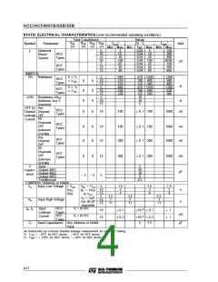
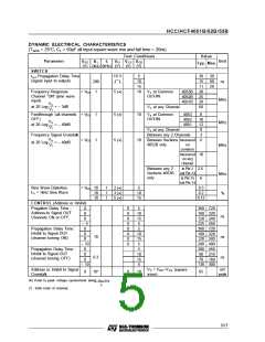
DYNAMIC ELECTRICAL CHARACTERISTICS
(Tamb = 25°C, CL = 50pF all input square wave rise and fall time = 20ns)
Test Conditions
Value
Parameter
SWITCH
Unit
VEE R L
(V) (kΩ) (kHz) (V)
fi
VIS VSS VDD
Typ. Max.
(V)
(V)
tp d Propagation Delay Time
(signal input to output)
10 V
__
5
30
15
11
30
25
20
60
30
60
20
_
_
10
15
10
200
1
I
I
ns
Frequency Response
Channel ”ON” (sine wave
input)
= V
5 (•)
Vo at Common
OUT/IN
4053B
4052B
4051B
SS
MHz
Vo
__
VI
at 20 Log
= – 3dB
Vo at any Channel
Feedthrough (all channels = V
1
1
5 (•)
10
10
Vo at Common
OUT/IN
4053
4052
4051
8
10
12
8
3
6
SS
OFF)
Vo
__
VI
MHz
MHz
at 20 Log
= – 40dB
Vo at any Channel
Between any 2 Channels
Between Sections measured
4052B only
Frequency Signal Crosstalk
Vo
= V
5 (•)
__
SS
at 20 Log
= – 40dB
on
VI
common
measured 10
on any
channel
Between any 2
Sections 4053B
only
in Pin 2 2.5
out Pin 14
MHz
%
in Pin 15
6
out Pin 14
Sine Wave Distortion
fis = 1kHz Sine Wave
= V
10
10
10
1
1
1
2 (•)
3 (•)
5 (•)
5
10
15
0.3
0.2
SS
0.12
CONTROL (Address or Inhibit)
Progation Delay Time :
Address-to Signal OUT
Channels ON or OFF
0
0
0
– 5
0
0
0
– 10
0
0
0
0
0
0
0
0
0
0
0
5
10
15
5
360 720
160 320
120 240
225 450
360 720
160 320
120 240
200 400
200 450
90 210
70 160
130 300
ns
ns
ns
Propagation Delay Time :
Inhibit to Signal OUT
(channel turning ON)
5
10
15
5
10
Propagation Delay Time :
Inhibit to Signal OUT
(channel turning OFF)
5
10
15
5
0.3
– 10
Address or Inhibit to Signal
Crosstalk
VC = VDD–VSS (square
wave)
mV
peak
0
10*
0
10
65
(•) Peak to peak voltage symmetrical about VDD-VEE
2
(*) Both ends of channel.
5/17

 STMICROELECTRONICS [ ST ]