PCF8575
REMOTE 16-BIT I2C AND SMBus I/O EXPANDER
WITH INTERRUPT OUTPUT
www.ti.com
SCPS121C–JANUARY 2005–REVISED OCTOBER 2006
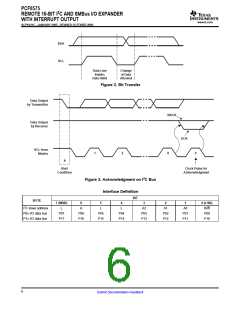
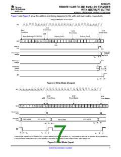
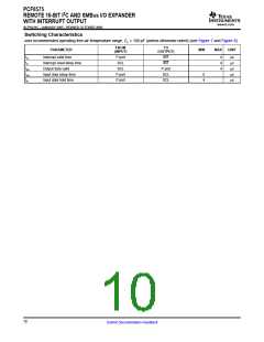
Figure 4 and Figure 5 show the address and timing diagrams for the write and read modes, respectively.
Integral Multiples of Two Bytes
SCL
1
6
2
3
4
6
7
8
1
2
3
4
5
7
8
1
2
3
4
5
6
7
8
5
ACK
From Slave
Start
Condition
ACK
From Slave
ACK
From Slave
R/W
Slave Address (PCF8575C)
Data to Port 0
Data to Port 1
SDA
S
0
1
0
0
A2 A1 A0
0
A
P07 P06
1
P00
A
P17
P10 A
P05
Write to
Port
Data A0
and B0
Valid
Data Output
Voltage
t
pv
P05 Output
Voltage
I
P05 Pullup
Output
OH
I
OHT
Current
INT
t
ir
Figure 4. Write Mode (Output)
SCL
1
6
2
3
4
6
7
8
1
2
3
4
5
7
8
1
2
3
4
5
6
7
8
5
ACK
From Master
ACK
From Slave
ACK
From Master
R/W
P07 P06 P05 P04 P03 P02 P01 P00
P17 P16 P15 P14 P13 P12 P11 P10
SDA
S
0
1
0
0
A2
1
A
A
P07 P06
A
A1 A0
Read From
Port
Data Into
Port
P17 to P10
P07 to P00
P17 to P10
P07 to P00
t
su
t
h
INT
t
ir
t
iv
t
ir
A low-to-high transition of SDA while SCL is high is defined as the stop condition (P). The transfer of data can be stopped at any moment by
a stop condition. When this occurs, data present at the latest ACK phase is valid (output mode). Input data is lost.
Figure 5. Read Mode (Input)
7
Submit Documentation Feedback

 TI [ TEXAS INSTRUMENTS ]