PCF8575
REMOTE 16-BIT I2C AND SMBus I/O EXPANDER
WITH INTERRUPT OUTPUT
www.ti.com
SCPS121C–JANUARY 2005–REVISED OCTOBER 2006
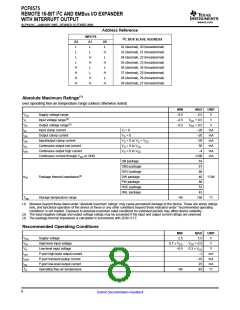
Electrical Characteristics
over recommended operating free-air temperature range (unless otherwise noted)
PARAMETER
TEST CONDITIONS
II = –18 mA
VCC
2.5 V to 5.5 V
VPOR
MIN TYP(1)
MAX
UNIT
V
VIK
Input diode clamp voltage
VPOR Power-on reset voltage(2)
–1.2
1.2
VI = VCC or GND, IO = 0
VO = GND
1.8
V
IOH P port
2.5 V to 5.5 V
2.5 V
–30
–300
µA
mA
IOHT P-port transient pullup current
SDA
High during ACK, VOH = GND
VOL = 0.4 V
–0.5
3
–1
VOL = 0.4 V
5
15
25
IOL
P port
2.5 V to 5.5 V
mA
VOL = 1 V
10
1.6
INT
VOL = 0.4 V
SCL, SDA
A0, A1, A2
P port
±5
±1
II
VI = VCC or GND
2.5 V to 5.5 V
µA
µA
IIHL
VI ≥ VCC or VI ≤ GND
2.5 V to 5.5 V
5.5 V
±400
200
75
100
30
VI = VCC or GND, IO = 0,
fscl = 400 kHz
Operating mode
Standby mode
3.6 V
2.7 V
20
50
ICC
µA
5.5 V
2.5
2.5
2.5
10
VI = VCC or GND, IO = 0, fscl = 0 kHz
3.6 V
10
2.7 V
10
One input at VCC – 0.6 V,
Other inputs at VCC or GND
∆ICC Supply current increase
2.5 V to 5.5 V
2.5 V to 5.5 V
200
µA
CI
SCL
VI = VCC or GND
3
3
4
7
7
pF
SDA
P port
Cio
VIO = VCC or GND
2.5 V to 5.5 V
pF
10
(1) All typical values are at nominal supply voltage (2.5-V, 3.3-V, or 5-V VCC) and TA = 25°C.
(2) The power-on reset circuit resets the I2C bus logic with VCC < VPOR and sets all I/Os to logic high (with current source to VCC).
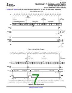
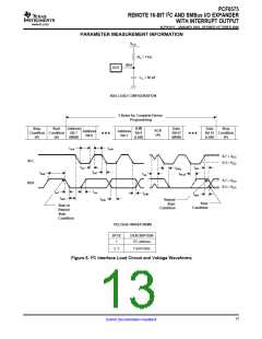
I2C Interface Timing Requirements
over recommended operating free-air temperature range (unless otherwise noted) (see Figure 6)
MIN
MAX UNIT
fscl
tsch
tscl
tsp
I2C clock frequency
I2C clock high time
I2C clock low time
I2C spike time
I2C serial data setup time
I2C serial data hold time
I2C input rise time
I2C input fall time
I2C output fall time
I2C bus free time between Stop and Start
I2C start or repeated Start condition setup
I2C start or repeated Start condition hold
I2C Stop condition setup
Valid-data time
400
kHz
µs
µs
ns
ns
ns
ns
ns
ns
µs
µs
µs
µs
µs
pF
0.6
1.3
50
tsds
tsdh
ticr
100
0
(1)
20 + 0.1Cb
300
300
300
(1)
ticf
20 + 0.1Cb
tocf
tbuf
tsts
tsth
tsps
tvd
10-pF to 400-pF bus
1.3
0.6
0.6
0.6
SCL low to SDA output valid
1.2
Cb
I2C bus capacitive load
400
(1) Cb = total bus capacitance of one bus line in pF
9
Submit Documentation Feedback

 TI [ TEXAS INSTRUMENTS ]