TL594
PULSE-WIDTH-MODULATION CONTROL CIRCUITS
SLVS052C – APRIL 1988 – REVISED JULY 1999
†
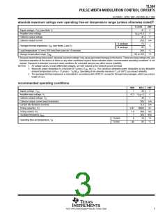
absolute maximum ratings over operating free-air temperature range (unless otherwise noted)
TL594X
41
UNIT
V
Supply voltage, V
CC
(see Note 1)
Amplifier input voltage
Collector output voltage
Collector output current
V
CC
+0.3
41
V
V
250
73
mA
D package
N package
Package thermal impedance, θ (see Notes 2 and 3)
°C
JA
88
Lead temperature 1,6 mm (1/16 inch) from case for 10 seconds
260
°C
°C
Storage temperature range, T
stg
–65 to 150
†
Stresses beyond those listed under “absolute maximum ratings” may cause permanent damage to the device. These are stress ratings only, and
functional operation of the device at these or any other conditions beyond those indicated under “recommended operating conditions” is not
implied. Exposure to absolute-maximum-rated conditions for extended periods may affect device reliability.
NOTES: 1. All voltage values, except differential voltages, are with respect to the network ground terminal.
2. Maximum power dissipation is a function of T (max), θ , and T . The maximum allowable power dissipation at any allowable
J
JA
A
ambient temperature is P = (T (max) – T )/θ . Operating at the absolute maximum T of 150°C can impact reliability.
D
J
A
JA
J
3. The package thermal impedance is calculated in accordance with JESD 51, except for through-hole packages, which use a trace
length of zero.
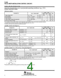
recommended operating conditions
MIN
7
MAX
UNIT
V
Supply voltage, V
CC
40
Amplifier input voltage, V
–0.3
V
CC
–2
40
V
I
Collector output voltage, V
V
O
Collector output current (each transistor)
200
0.3
mA
mA
nF
kΩ
kHz
°C
Current into feedback terminal
Timing capacitor, C
0.47
1.8
1
10000
500
300
70
T
Timing resistor, R
T
Oscillator frequency, f
osc
TL594C
TL594I
0
Operating free-air temperature, T
A
–40
85
°C
3
POST OFFICE BOX 655303 • DALLAS, TEXAS 75265

 TI [ TEXAS INSTRUMENTS ]