TMC2160 DATASHEET (Rev. 1.02 / 2018-NOV-19)
11
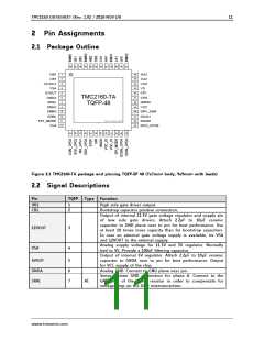
2 Pin Assignments
2.1 Package Outline
36
35
34
33
32
31
30
29
28
27
26
25
1
HB1
HA2
2
CB1
CA2
3
12VOUT
VCP
4
VSA
VS
5
5VOUT
CPI
6
TMC2160-TA
GNDA
CPO
7
SRAL
GNDD
VCC
TQFP-48
8
SRAH
9
SRBH
DRV_ENN
DIAG1
DIAG0
DCO_CFG6
10
SRBL
PAD = GNDD, GNDP
11
12
TST_MODE
CLK
Figure 2.1 TMC2160-TA package and pinning TQFP-EP 48 (7x7mm² body, 9x9mm² with leads)
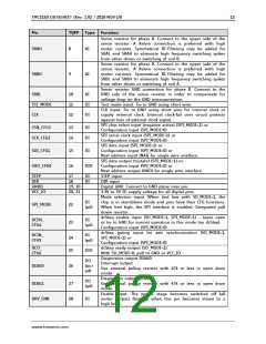
2.2 Signal Descriptions
Pin
TQFP Type Function
HB1
CB1
1
2
High side gate driver output.
Bootstrap capacitor positive connection.
Output of internal 11.5V gate voltage regulator and supply pin
of low side gate drivers. Attach 2.2µF to 10µF ceramic
capacitor to GND plane near to pin for best performance. Use
at least 10 times more capacity than for bootstrap capacitors.
In case an external gate voltage supply is available, tie VSA
and 12VOUT to the external supply.
12VOUT
VSA
3
4
Analog supply voltage for 11.5V and 5V regulator. Normally
tied to VS. Provide a 100nF filtering capacitor.
Output of internal 5V regulator. Attach 2.2µF to 10µF ceramic
capacitor to GNDA near to pin for best performance. Output
for VCC supply of the chip.
5VOUT
GNDA
SRAL
5
6
7
Analog GND. Connect to GND plane near pin.
Sense resistor GND connection for phase A. Connect to the
GND side of the sense resistor in order to compensate for
voltage drop on the GND interconnection.
AI
www.trinamic.com

 TRINAMIC [ TRINAMIC MOTION CONTROL GMBH & CO. KG. ]