TMC2160 DATASHEET (Rev. 1.02 / 2018-NOV-19)
12
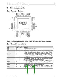
Pin
TQFP Type Function
Sense resistor for phase A. Connect to the upper side of the
sense resistor. A Kelvin connection is preferred with high
motor currents. Symmetrical RC-Filtering may be added for
SRAL and SRAH to eliminate high frequency switching spikes
from other drives or switching of coil B.
SRAH
8
AI
Sense resistor for phase B. Connect to the upper side of the
sense resistor. A Kelvin connection is preferred with high
motor currents. Symmetrical RC-Filtering may be added for
SRBL and SRBH to eliminate high frequency switching spikes
from other drives or switching of coil A.
SRBH
9
AI
Sense resistor GND connection for phase B. Connect to the
GND side of the sense resistor in order to compensate for
voltage drop on the GND interconnection.
Test mode input. Tie to GND using short wire.
CLK input. Tie to GND using short wire for internal clock or
supply external clock. Internal clock-fail over circuit protects
against loss of external clock signal.
SRBL
10
11
12
AI
DI
DI
TST_MODE
CLK
SPI chip select input (negative active) (SPI_MODE=1) or
Configuration input (SPI_MODE=0)
SPI serial clock input (SPI_MODE=1) or
CSN_CFG3
SCK_CFG2
13
14
DI
DI
Configuration input (SPI_MODE=0)
SPI data input (SPI_MODE=1) or
SDI_CFG1
SDO_CFG0
15
16
DI
Configuration input (SPI_MODE=0) or
Next address input (NAI) for single wire interface.
SPI data output (tristate) (SPI_MODE=1) or
Configuration input (SPI_MODE=0) or
DIO
Next address output (NAO) for single wire interface.
STEP
DIR
17
18
DI
DI
STEP input
DIR input
GNDD
VCC_IO
19, 30
20, 21
Digital GND. Connect to GND plane near pin.
3.3V to 5V IO supply voltage for all digital pins.
Mode selection input. When tied low with SD_MODE=1, the
chip is in standalone mode and pins have their CFG functions.
When tied high, the SPI interface is enabled. Integrated pull
down resistor.
dcStep enable input (SD_MODE=1, SPI_MODE=1) – leave open
or tie to GND for normal operation in this mode (no dcStep).
Configuration input (SPI_MODE=0)
DI
(pd)
SPI_MODE
22
23
DCEN_
CFG4
DI
(pd)
dcStep gating input for axis synchronization (SD_MODE=1,
SPI_MODE=1) or
Configuration input (SPI_MODE=0)
dcStep ready output (SD_MODE=1).
With SD_MODE=0, pull to GND or VCC_IO
DCIN_
CFG5
DI
(pd)
24
25
DCO_
CFG6
DIO
Diagnostics output DIAG0.
Interrupt output
Use external pullup resistor with 47k or less in open drain
mode.
DO
(pu+
pd)
DIAG0
26
Diagnostics output DIAG1.
Use external pullup resistor with 47k or less in open drain
mode.
DO
(pd)
DIAG1
27
28
Enable input. The power stage becomes switched off (all
motor outputs floating) when this pin becomes driven to a
high level.
DRV_ENN
DI
www.trinamic.com

 TRINAMIC [ TRINAMIC MOTION CONTROL GMBH & CO. KG. ]