VRAM
SMJ44C251B
MT42C4256
Austin Semiconductor, Inc.
DESCRIPTION
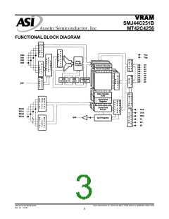
The SMJ44C251B/MT42C4256 multiport video RAM is a half and a low half. While one half is being read out of the SAM
high-speed, dual-ported memory device. It consists of a port, the other half can be loaded from the memory array. For
dynamic random-access memory (DRAM) organized as 262144 applications not requiring real-time register reload (for example,
words of 4 bits each interfaced to a serial-data register or serial- reloads done during CRT retrace periods), the single-register
access memory (SAM) organized as 512 words of 4 bits each. mode of operation is retained to simplify design. The SAM can
The SMJ44C251B/MT42C4256 supports three types of also be configured in input mode, accepting serial data from an
operation: random access to and from the DRAM, serial access external device. Once the serial register within the SAM is
to and from the serial register, and bidirectional transfer of data loaded, its contents can be transferred to the corresponding
between any row in the DRAM and the serial register. Except column positions in any row in memory in a single memory
during transfer operations, the SMJ44C251B/MT42C4256 can cycle.
be accessed simultaneously and asynchronously from the
DRAM and SAM ports.
The SAM port is designed for maximum performance. Data
can be input to or accessed from the SAM at serial rates up to
During a transfer operation, the 512 columns of the DRAM 33 MHz. During the split-register mode of operation, internal
are connected to the 512 positions in the serial data register. circuitry detects when the last bit position is accessed from the
The 512 × 4-bit serial-data register can be loaded from the active half of the register and immediately transfers control to
memory row (transfer read), or the contents of the 512 × 4-bit the opposite half. A separate output, QSF, is included to
serial-data register can be written to the memory row (transfer indicate which half of the serial register is active at any given
write).
The SMJ44C251B/MT42C4256 is equipped with several
time in the split-register mode.
All inputs, outputs, and clock signals on the SMJ44C251B/
features designed to provide higher system-level bandwidth MT42C4256 are compatible with Series 54 TTLdevices.All ad-
and to simplify design integration on both the DRAM and SAM dress lines and data-in lines are latched on-chip to simplify
ports. On the DRAM port, greater pixel draw rates can be system design. All data-out lines are unlatched to allow greater
achieved by the device’s 4 × 4 block-write mode. The block- system flexibility.
write mode allows four bits of data (present in an on-chip color-
Enhanced page-mode operation allows faster memory
data register) to be written to any combination of four adjacent access by keeping the same row address while selecting
column-address locations. As many as 16 bits of data can be random column addresses. The time for row-address setup,
written to memory during each CAS cycle time. Also on the row-address hold, and address multiplex is eliminated, and a
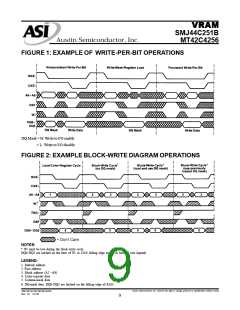
DRAM port, a write mask or a write-per-bit feature allows mask- memory cycle time reduction of up to 3× can be achieved,
ing any combination of the four input/outputs on any write compared to minimum RAS cycle times. The maximum number
cycle. The persistent write-per-bit feature uses a mask register of columns that can be accessed is determined by the maximum
that, once loaded, can be used on subsequent write cycles. The RAS low time and page-mode cycle time used. The
mask register eliminates having to provide mask data on every SMJ44C251B/MT42C4256 allows a full page (512 cycles) of
mask-write cycle.
information to be accessed in read, write, or read-modify-write
The SMJ44C251B/MT42C4256 offers a split-register mode during a single RAS-low period using relatively conser-
transfer read (DRAM to SAM) feature for the serial tester (SAM vative page-mode cycle times.
port). This feature enables real-time register reload
The SMJ44C251B/MT42C4256 employs state-of-the-art
implementation for truly continuous serial data streams without technology for very high performance combined with improved
critical timing requirements. The register is divided into a high reliability.
Austin Semiconductor, Inc. reserves the right to change products or specifications without notice.
SMJ44C251B/MT42C4256
Rev. 0.1 12/03
2

 AUSTIN [ AUSTIN SEMICONDUCTOR ]