VRAM
SMJ44C251B
MT42C4256
Austin Semiconductor, Inc.
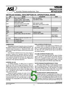
WRITE-MASK SELECT, WRITE ENABLE (W\)
(continued)
For transfer operation, W\ selects either a read-transfer
operation (DRAM to SAM) or a write-transfer operation (SAM
to DRAM). During a transfer cycle, if W is high when RAS\
falls, a read transfer occurs; if W is low, a write transfer occurs.
serial-output mode, data in SAM is accessed from the least
significant bit to the most significant bit. The data registers
operate modulo 512; so after bit 511 is accessed, the next bits to
be accessed are 00, 01, 02, etc. If the previous transfer cycle was
either a write transfer or a pseudo transfer, the data register is in
serial-input mode and signal data can be input to the register.
SPECIAL FUNCTION SELECT (DSF)
SERIAL CLOCK (SC)
DSF is latched on the falling edge of RAS\ or CAS\, similar
to an address. DSF determines which of the following functions
are invoked on a particular cycle:
Serial data is accessed in or out of the data register on the
rising edge of SC. The SMJ44C251B/MT42C4256 is designed
to work with a wide range of clock-duty cycles to simplify
system design. There is no refresh requirement because the
data registers that comprise the SAM are static. There is also
no minimum SC clock operating frequency.
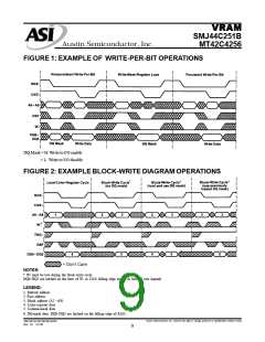
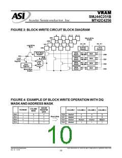
• Persistent write-per-bit
• Block write
• Split-register transfer read
• Mask-register load for the persistent write-per-bit mode
• Color-register load for the block-write mode
SERIAL ENABLE (SE\)
During serial-access operations SE\ is used as an enable/
disable for SDQ in both the input and output modes. If SE\ is
held as RAS\ falls during a write-transfer cycle, a pseudo-
transfer write occurs. There is no actual transfer, but the data
register switches from the output mode to the input mode.
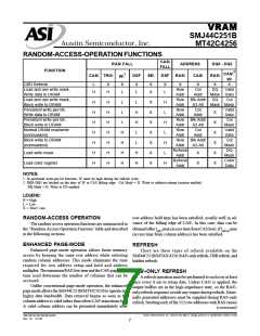
DRAM DATAI/O, WRITE-MASK DATA (DQ0–DQ3)
DRAM data is written via DQ terminals during a write or
read-modify-write cycle. In an early-write cycle, W\ is brought
low prior to CAS\ and the data is strobed in by CAS\ with data
setup and hold times referenced to this signal. In a delayed-
write or read-modify-write cycle, W\ is brought low after CAS\
and the data is strobed in by W\ with data setup and hold times
referenced to this signal.
The 3-state DQ output buffers provide direct TTL
compatibility (no pullup resistors) with a fanout of two Series 54
TTL loads. Data out is the same polarity as data in. The outputs
are in the high-impedance (floating) state as long as CAS\ and
TRG\ are held high. Data does not appear at the outputs until
both CAS\ and TRG\ are brought low. Once the outputs are
valid, they remain valid while CAS\ and TRG\ are low. CAS\ or
TRG\ going high returns the outputs to the high-impedance
state. In a register-transfer operation, the DQ outputs remain in
the high-impedance state for the entire cycle.
NO CONNECT/GROUND (NC/GND)
NC/GND is reserved for the manufacturer’s test operation.
It is an input and should be tied to system ground or left
floating for proper device operation.
SPECIAL FUNCTION OUTPUT (QSF)
During split-register operation the QSF output indicates
which half of the SAM is being accessed. When QSF is low, the
serial-address pointer is accessing the lower (least significant)
256 bits of SAM. When QSF is high, the serial-address pointer
is accessing the higher (most significant) 256 bits of SAM. QSF
changes state upon crossing the boundary between the two
SAM halves in the split-register mode.
During normal transfer operations QSF changes state upon
completing a transfer cycle. This state is determined
by the tap point being loaded during the transfer cycle.
The write-per-bit mask is latched into the device via the
random DQ terminals by the falling edge of RAS\. This mask
selects which of the four random I/Os are written.
POWER UP
SERIAL DATAI/O (SDQ0–SDQ3)
To achieve proper device operation, an initial pause of
200ms is required after power-up, followed by a minimum of
eight RAS\ cycles or eight CBR cycles, a memory-to-register
transfer cycle, and two SC cycles.
Serial inputs and serial outputs share common I/O
terminals. Serial-input or serial-output mode is determined by
the previous transfer cycle. If the previous transfer cycle was a
read transfer, the data register is in serial-output mode. While in
Austin Semiconductor, Inc. reserves the right to change products or specifications without notice.
SMJ44C251B/MT42C4256
Rev. 0.1 12/03
6

 AUSTIN [ AUSTIN SEMICONDUCTOR ]