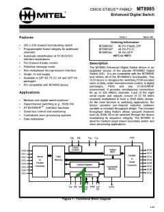
MT8985
time slot interchange functions with different
throughput delay capabilities on a per-channel basis.
For voice applications, the variable delay mode can
be selected ensuring minimum throughput delay
between input and output data. In multiple or
grouped channel data applications, the constant
delay mode can be selected maintaining the integrity
of the information through the switch.
three-state condition. In addition, the Connect
Memory High provides one bit to allow the user to
control the state of the CSTo output pin.
If an output channel is set to three-state condition,
the TDM serial stream output will be placed in high
impedance during that channel time. In addition to
the per-channel three-state control, all channels on
the TDM outputs can be placed in high impedance at
one time by pulling the ODE input pin in LOW. This
overrides the individual per-channel programming on
the Connect Memory High bits.
Data to be output on the serial streams may come
from two sources: Data Memory or Connect Memory.
Locations in the Connect Memory, which is split into
HIGH and LOW parts, are associated with particular
ST-BUS output streams. When a channel is due to
be transmitted on an ST-BUS output, the data for the
channel can either be switched from an ST-BUS
input (connection mode) or it can be originated from
the microprocessor (message mode). If a channel is
configured in connection mode, the source of the
output data is the Data Memory. If a channel is
configured in message mode, the source of the
output data is the Connect Memory Low. Data
destined for a particular channel on the serial output
stream is read from the Data or Connect Memory
Low during the previous channel time slot. This
allows enough time for memory access and internal
parallel to serial conversion.
The Connect Memory data is received via the
Microprocessor Interface at D0-D7 lines. The
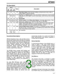
addressing of the MT8985 internal registers, Data
and Connect memories is performed through
address input pins and some bits of the device's
Control register. The higher order address bits come
from the Control register, which may be written or
read through the microprocessor interface. The lower
order address bits come directly from the external
address line inputs. For details on the device
addressing, see Software Control and Control
register description.
Serial Interface Timing
Connection and Message Modes
The MT8985 master clock (C4i) is a 4.096 MHz
allowing serial data link configuration at 2.048 Mb/s
In connection mode, the addresses of input source
for all output channels are stored in the Connect
memory Low. The Connect Memory Low locations
are mapped to each location corresponding to an
output 64 kb/s channel. The contents of the Data
memory at the selected address are then transferred
to the parallel to serial converters. By having the
output channel to specify the input channel through
the connect memory, the user can route the same
input channel to several output channels, allowing
broadcasting facility in the switch.
to
be
implemented.
The
MT8985
frame
synchronization pulse can be formatted according to
ST-BUS or GCI interface specifications; i.e., the
frame pulse can be active in HIGH (GCI) or LOW
(ST-BUS). The MT8985 device automatically detects
the presence of an input frame pulse and identifies
the type of backplane present on the serial interface.
Upon determining the correct interface connected to
the serial port, the internal timing unit establishes the
appropriate serial data bit transmit and sampling
edges. In ST-BUS mode, every second falling edge
of the 4.096 MHz clock marks a bit boundary and the
input data is clocked in by the rising edge, three
quarters of the way into the bit cell. In GCI mode,
every second rising edge of the 4.096 MHz clock
marks the bit boundary while data sampling is
performed during the falling edge, at three quarters
of the bit boundaries.
In message mode the CPU writes data to the
Connect Memory Low locations which correspond to
the output link and channel number. The contents of
the Connect Memory Low are transferred to the
parallel to serial converter one channel before it is to
be output. The Connect Memory Low data is
transmitted each frame to the output until it is
changed by the CPU.
Delay through the MT8985
The per-channel functions available in the MT8985
are controlled by the Connect Memory High bits,
which determine whether individual output channels
are selected into specific conditions such as:
message or connection mode, variable or constant
throughput delay modes, output drivers enabled or in
The transfer of information from the input serial
streams to the output serial streams results in a
delay through the MT8985 device. The delay through
the MT8985 device varies according to the mode
selected in the V/C bit of the connect memory high.
2-48

 MITEL [ MITEL NETWORKS CORPORATION ]