MT8985
Variable Delay mode
output frame N+2. In Constant Delay mode, the
device throughput delay is calculated according to
the following formula:
The delay in this mode is dependent only on the
combination of source and destination channels and
it is not dependent on the input and output streams.
The minimum delay achievable in the MT8985 device
is 3 time slots. In the MT8985 device, the information
that is to be output in the same channel position as
the information is input (position n), relative to frame
pulse, will be output in the following frame (channel
n, frame n+1). The same occurs if the input channel
has to be output in the two channels succeeding
(n+1 and n+2) the channel position as the
information is input.
DELAY = [32 + (32 - IN) + (OUT - 1)];
(expressed in number of time slots)
Where:
IN is the number of the input time slot
(from 1 to 32).
OUT is the number of the output time slot
(from 1 to 32).
Microprocessor Port
The information switched to the third timeslot after
the input has entered the device (for instance, input
channel 0 to output channel 3 or input channel 30 to
output channel 1), is always output three channels
later.
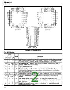
The MT8985 microprocessor port has pin
compatibility with Mitel MT8980 Digital Switch device
providing a non-multiplexed bus architecture. The
parallel port consists of an 8 bit parallel data bus
(D0-D7), six address input lines (A0-A5) and four
control lines (CS, DS, R/W and DTA). This parallel
microport allows the access to the Control registers,
Connection Memory High, Connection Memory Low
and the Data Memory. All locations are read/written
except for the data memory which can be read only.
Any switching configuration that provides three or
more timeslots between input and output channels,
will have a throughput delay equal to the difference
between the output and input channels; i.e., the
throughput delay will be less than one frame. Table 1
shows the possible delays for the MT8985 device in
Variable Delay mode:
Accesses from the microport to the connection
memory and the data memory are multiplexed with
accesses from the input and output TDM ports. This
can cause variable Data Acknowledge delays (DTA).
In the MT8985 device, the DTA output provides a
maximum acknowledgement delay of 800 ns for
read/write operations in the Connection Memory.
However, for operations in the Data Memory
(Message Mode), the maximum acknowledgement
delay can be 1220 ns.
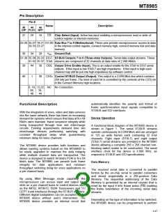
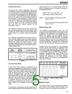
Input
Channel
Output
Channel
Throughput Delay
n
m=n, n+1 or
n+2
m-n + 32 timeslots
n
n
m>n+2
m<n
m-n time slots
32-(n-m) time slots
Table 1
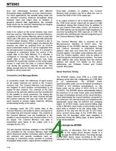
A5 A4 A3 A2 A1 A0
LOCATION
Constant Delay Mode
0
1
1
1
1
1
1
1
1
X
0
0
•
•
•
•
•
1
X
0
0
•
•
•
•
•
1
X
0
0
•
•
•
•
•
1
0
0
0
•
•
•
•
•
1
0
0
1
•
•
•
•
•
1
ControlRegister
Channel 0
Channel 1
In this mode frame integrity is maintained in all
switching configurations by making use of a multiple
Data-Memory buffer technique where input channels
written in any of the buffers during frame N will be
read out during frame N+2. In the MT8985, the
minimum throughput delay achiev-able in Constant
Delay mode will be 32 time slots; for example, when
input time slot 32 (channel 31) is switched to output
time slot 1 (channel 0). Likewise, the maximum delay
is achieved when the first time slot in a frame
(channel 0) is switched to the last time slot in the
frame (channel 31), resulting in 94 time slots of
delay.
•
•
•
•
•
Channel 31
Figure 3 - Address Memory Map
Note: "x" Don’t care
Software Control
The address lines on the microprocessor interface
give access to the MT8985 internal registers and
memories. If the A5,A1,A0 address line inputs are
To summarize, any input time slot from input frame N
will be always switched to the destination time slot on
2-49

 MITEL [ MITEL NETWORKS CORPORATION ]