DC and AC parameters
NAND01G-B2B, NAND02G-B2C
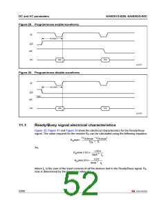
Figure 29. Program/erase enable waveforms
W
tVHWH
WP
RB
I/O
80h
10h
ai12477
Figure 30. Program/erase disable waveforms
W
tVLWH
WP
High
RB
I/O
80h
10h
ai12478
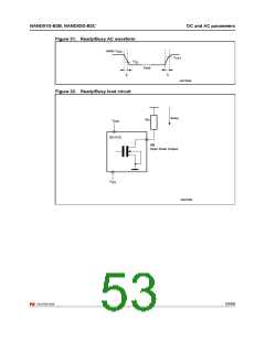
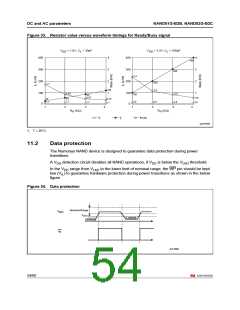
11.1
Ready/Busy signal electrical characteristics
Figure 32, Figure 31 and Figure 33 show the electrical characteristics for the Ready/Busy
signal. The value required for the resistor R can be calculated using the following equation:
P
(
–
)
V
V
DDmax
OLmax
+ I
R min= -------------------------------------------------------------
P
I
L
OL
So,
1.85V
R min(1.8V)= ---------------------------
P
+
3mA
I
L
3.2V
R min(3V)= ---------------------------
P
+
8mA
I
L
where I is the sum of the input currents of all the devices tied to the Ready/Busy signal. R
L
P
max is determined by the maximum value of t .
r
52/60

 NUMONYX [ NUMONYX B.V ]