DC and AC parameters
NAND01G-B2B, NAND02G-B2C
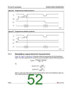
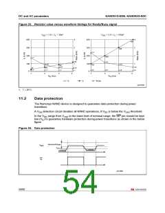
Figure 33. Resistor value versus waveform timings for Ready/Busy signal
V
= 1.8V, C = 30pF
V = 3.3V, C = 100pF
DD L
DD
L
400
300
200
400
300
200
4
3
2
4
3
2
400
300
2.4
200
1.7
120
1.2
100
0
1
100
0
1
0.85
0.8
100
3.6
90
0.57
0.6
3.6
60
1.7
0.43
1.7
30
1.7
3.6
3.6
1.7
1
2
3
4
1
2
3
4
R
(KΩ)
R (KΩ)
P
P
t
t
r
ibusy
f
ai07565B
1. T = 25°C.
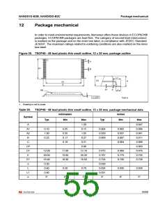
11.2
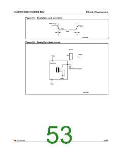
Data protection
The Numonyx NAND device is designed to guarantee data protection during power
transitions.
A V detection circuit disables all NAND operations, if V is below the V threshold.
LKO
DD
DD
In the V range from V
to the lower limit of nominal range, the WP pin should be kept
DD
LKO
low (V ) to guarantee hardware protection during power transitions as shown in the below
IL
figure.
Figure 34. Data protection
Nominal Range
V
DD
V
LKO
Locked
Locked
W
Ai11086
54/60

 NUMONYX [ NUMONYX B.V ]