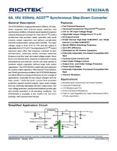
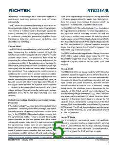
RT6236A/B
Ordering Information
RT6236A/B
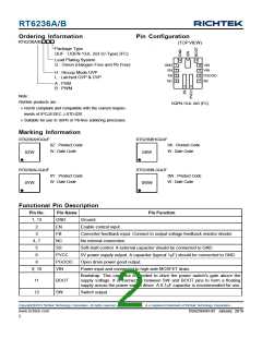
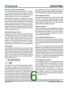
Pin Configuration
(TOP VIEW)
Package Type
QUF : UQFN-13JL 2x3 (U-Type) (FC)
13
12
11
Lead Plating System
1
2
3
4
G : Green (Halogen Free and Pb Free)
10
9
GND
EN
VIN
VIN
H : Hiccup Mode UVP
L : Latched OVP & UVP
8
FB
PGOOD
NC
7
NC
A : PSM
B : PWM
5
6
Note :
Richtek products are :
UQFN-13JL 2x3 (FC)
RoHS compliant and compatible with the current require-
ments of IPC/JEDEC J-STD-020.
Suitable for use in SnPb or Pb-free soldering processes.
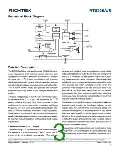
Marking Information
RT6236AHGQUF
RT6236BHGQUF
0XW
0Z : Product Code
0X : Product Code
W : Date Code
W : Date Code
0ZW
RT6236ALGQUF
0Y : Product Code
RT6236BLGQUF
0WW
0W : Product Code
W : Date Code
W : Date Code
0YW
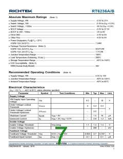
Functional Pin Description
Pin No.
Pin Name
GND
EN
Pin Function
1, 13
Ground.
2
3
Enable control input.
FB
Converter feedback input. Connect to output voltage feedback resistor divider.
No internal connection.
4, 7
5
NC
SS
Soft-start control. A external capacitor should be connected to GND.
5V power supply output. A capacitor (typical 1F) should be connected to GND.
Open drain power good output.
6
PVCC
PGOOD
VIN
8
9, 10
Power input and connected to high-side MOSFET drain.
Bootstrap. This capacitor is needed to drive the power switch's gate above the
supply voltage. It is connected between SW and BOOT pins to form a floating
supply across the power switch driver. A 0.1F capacitor is recommended for use.
11
12
BOOT
SW
Switch output.
Copyright 2018 Richtek Technology Corporation. All rights reserved.
©
is a registered trademark of Richtek Technology Corporation.
www.richtek.com
2
DS6236A/B-03 January 2018

 RICHTEK [ RICHTEK TECHNOLOGY CORPORATION ]