256M GDDR3 SDRAM
K4J55323QG
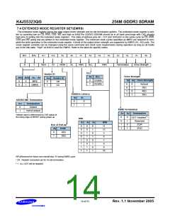
7.4 EXTENDED MODE REGISTER SET(EMRS)
The extended mode register stores the data output driver strength and on-die termination options. The extended mode register is writ-
ten by asserting low on CS, RAS, CAS, WE and high on BA0(The GDDR3 SDRAM should be in all bank precharge with CKE already
high prior to writing into the extended mode register). The state of address pins A0 ~ A11 and BA0,BA1 in the same cycle as CS, RAS,
CAS and WE going low are written in the extended mode register. The minimum clock cycles specified as tMRD are required to com-
plete the write operation in the extended mode register. 4 kinds of the output driver strength are supported by EMRS (A1, A0) code. The
mode register contents can be changed using the same command and clock cycle requirements during operation as long as all banks
are in the idle state. "High" on BA0 is used for EMRS. Refer to the table for specific codes.
BA1
0
BA0
1
A11
A10
ID
A9
A8
A7
A6
A5
A4
A3
A2
A1
A0
Term
RON
AL
tWR
DLL
tWR
Termination
Drive Strength
DLL
Vendor ID
A10 Vendor ID
Drive Strength
A1 A0 Drive Strength
A6
0
1
DLL
Enable
Disable
BA1 BA0 An ~ A0
0
0
0
1
MRS
EMRS
0
1
Off
On
0
0
1
1
0
1
0
1
Autocal
30Ω
40Ω
Additive Latency
50Ω
A8
0
1
AL
0
1
ADDR/CMD Termination
A11
0
Termination
Default
Data Termination
1
Half of default
A3
A2
Termination
Default value is determined by CKE status at
the rising edge of RESET during power-up
ODT Disabled*1
Reserved
ZQ/4
0
0
tWR
A7 A5 A4
0
1
1
0
tWR
11
13
5
6
7
8
9
10
Ron of Pull-up
0
0
0
0
1
1
1
1
0
0
1
1
0
0
1
1
0
1
0
1
0
1
0
1
1
1
ZQ/2
A9
0
RON
40Ω
60Ω
1
RFU(Reserved for future use) should stay "0" during EMRS cycle
* ZQ : Resistor connection pin for On-die termination
* 1 : ALL ODT will be disabled
14 of 53
Rev. 1.1 November 2005

 SAMSUNG [ SAMSUNG ]