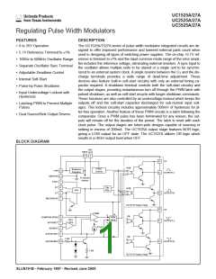
UC1525A/27A
UC2525A/27A
UC3525A/27A
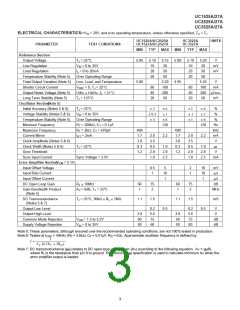
ABSOLUTE MAXIMUM RATINGS(Note 1)
RECOMMENDED OPERATING CONDITIONS
(Note 3)
Supply Voltage, (+VIN). . . . . . . . . . . . . . . . . . . . . . . . . . . . +40V
Collector Supply Voltage (VC) . . . . . . . . . . . . . . . . . . . . . . +40V
Logic Inputs . . . . . . . . . . . . . . . . . . . . . . . . . . . . –0.3V to +5.5V
Analog Inputs . . . . . . . . . . . . . . . . . . . . . . . . . . . . –0.3V to +VIN
Output Current, Source or Sink . . . . . . . . . . . . . . . . . . . 500mA
Reference Output Current . . . . . . . . . . . . . . . . . . . . . . . . 50mA
Oscillator Charging Current . . . . . . . . . . . . . . . . . . . . . . . . 5mA
Power Dissipation at TA = +25°C (Note 2). . . . . . . . . . 1000mW
Power Dissipation at TC = +25°C (Note 2) . . . . . . . . . 2000mW
Operating Junction Temperature . . . . . . . . . . –55°C to +150°C
Storage Temperature Range . . . . . . . . . . . . . –65°C to +150°C
Lead Temperature (Soldering, 10 seconds) . . . . . . . . . +300°C
Note 1: Values beyond which damage may occur.
Input Voltage (+VIN) . . . . . . . . . . . . . . . . . . . . . . . +8V to +35V
Collector Supply Voltage (VC). . . . . . . . . . . . . . . +4.5V to +35V
Sink/Source Load Current (steady state) . . . . . . . . 0 to 100mA
Sink/Source Load Current (peak) . . . . . . . . . . . . . . 0 to 400mA
Reference Load Current . . . . . . . . . . . . . . . . . . . . . . 0 to 20mA
Oscillator Frequency Range. . . . . . . . . . . . . . 100Hz to 400kHz
Oscillator Timing Resistor . . . . . . . . . . . . . . . . . . 2kΩ to 150kΩ
Oscillator Timing Capacitor . . . . . . . . . . . . . . . .001µF to .01µF
Dead Time Resistor Range . . . . . . . . . . . . . . . . . . . . 0 to 500Ω
Operating Ambient Temperature Range
UC1525A, UC1527A . . . . . . . . . . . . . . . . . . –55°C to +125°C
UC2525A, UC2527A . . . . . . . . . . . . . . . . . . . –25°C to +85°C
UC3525A, UC3527A . . . . . . . . . . . . . . . . . . . . . 0°C to +70°C
Note 3: Range over which the device is functional and parame-
ter limits are guaranteed.
Note 2: Consult packaging Section of Databook for thermal
limitations and considerations of package.
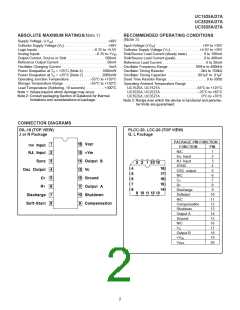
CONNECTION DIAGRAMS
DIL-16 (TOP VIEW)
J or N Package
PLCC-20, LCC-20 (TOP VIEW)
Q, L Package
PACKAGE PIN FUNCTION
FUNCTION
N/C
PIN
1
Inv. Input
N.I. Input
SYNC
2
3
4
OSC. output
N/C
5
6
CT
7
RT
8
Discharge
Softstart
N/C
Compensation
Shutdown
Output A
Ground
N/C
9
10
11
12
13
14
15
16
17
18
19
20
VC
Output B
+VIN
VREF
2

 TI [ TEXAS INSTRUMENTS ]