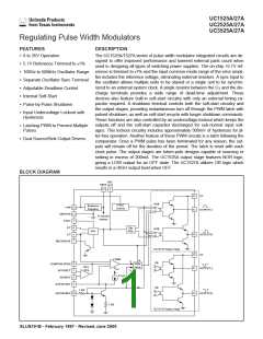
UC1525A/27A
UC2525A/27A
UC3525A/27A
ELECTRICAL CHARACTERISTICS:+VIN = 20V, and over operating temperature, unless otherwise specified, TA = TJ.
UC1525A/UC2525A
UC1527A/UC2527A
UC3525A
UC3527A
UNITS
PARAMETER
PWM Comparator
TEST CONDITIONS
MIN
TYP
MAX
MIN
TYP
MAX
Minimum Duty-Cycle
0
0
%
%
V
Maximum Duty-Cycle (Note 6)
Input Threshold (Note 6)
45
49
0.9
3.3
.05
45
49
0.9
3.3
.05
Zero Duty-Cycle
Maximum Duty-Cycle
0.7
0.7
3.6
1.0
3.6
1.0
V
Input Bias Current (Note 5)
Shutdown Section
µA
Soft Start Current
V
V
SD = 0V, VSS = 0V
SD = 2.5V
25
50
0.4
0.8
0.4
0.2
80
0.7
1.0
1.0
0.5
25
50
0.4
0.8
0.4
0.2
80
0.7
1.0
1.0
0.5
µA
V
Soft Start Low Level
Shutdown Threshold
Shutdown Input Current
Shutdown Delay (Note 5)
To outputs, VSS = 5.1V, TJ = 25°C
SD = 2.5V
VSD = 2.5V, TJ = 25°C
0.6
0.6
V
V
mA
µs
Output Drivers(Each Output) (VC = 20V)
Output Low Level
Output High Level
I
SINK = 20mA
0.2
1.0
19
18
7
0.4
2.0
0.2
1.0
19
18
7
0.4
2.0
V
V
ISINK = 100mA
I
I
SOURCE = 20mA
SOURCE = 100mA
18
17
6
18
17
6
V
V
Under-Voltage Lockout
VC OFF Current (Note 7)
Rise Time (Note 5)
V
COMP and VSS = High
8
8
V
VC = 35V
200
600
300
200
600
300
µA
ns
ns
CL = 1nF, TJ = 25°C
CL = 1nF, TJ = 25°C
100
50
100
50
Fall Time (Note 5)
Total Standby Current
Supply Current
VIN = 35V
14
20
14
20
mA
Note 5: These parameters, although ensured over the recommended operating conditions, are not 100% tested in production.
Note 6: Tested at fOSC = 40kHz (RT = 3.6kW, CT = 0.01mF, RD = 0W)
Note 7: Collector off-state quiescent current measured at pin 13 with outputs low for UC1525A and high for UC1527A.
4

 TI [ TEXAS INSTRUMENTS ]