CY7C68300B/CY7C68301B
CY7C68320/CY7C68321
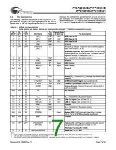
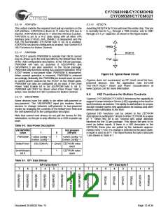
Table 5-1. AT2LP Pin Descriptions
Note: (Italics pin names denote pin functionality during CY7C68300A-compatibility mode) (continued)
56
56
100
Pin DefaultState
Type at Start-up
SSOP QFN TQFP
Pin Name
NC
Pin Description
N/A
22
N/A
15
28
29
30
No Connect.
SCL
O
Active for Clock signal for I2C interface (see section 5.3.2).
several ms at
23
16
SDA
I/O
Data signal for I2C interface (see section 5.3.2).
start-up.
N/A
N/A
31
32
NC
No Connect.
24
25
17
18
33
34
35
36
37
38
39
40
41
42
43
44
45
46
47
48
49
50
VCC
DD0
DD1
DD2
DD3
VCC
GND
NC
PWR
I/O[1]
I/O[1]
I/O[1]
I/O[1]
PWR
GND
NC
VCC. Connect to 3.3V power source.
Hi-Z
Hi-Z
Hi-Z
Hi-Z
ATA Data bit 0.
ATA Data bit 1.
ATA Data bit 2.
ATA Data bit 3.
VCC. Connect to 3.3V power source.
Ground.
26
19
27
20
28
21
N/A
N/A
N/A
N/A
N/A
N/A
29
N/A
N/A
N/A
N/A
N/A
N/A
22
No Connect.
GND
NC
Ground.
NC
No Connect.
GND
DD4
DD5
DD6
DD7
GND
VCC
GND
NC
Ground.
I/O[1]
I/O[1]
I/O[1]
I/O[1]
GND
PWR
GND
NC
Hi-Z
Hi-Z
Hi-Z
Hi-Z
ATA Data bit 4.
ATA Data bit 5.
ATA Data bit 6.
ATA Data bit 7.
Ground.
30
23
31
24
32
25
33
26
34
27
VCC. Connect to 3.3V power source.
Ground.
35
28
N/A
N/A
51
52
No Connect.
N/A
36
N/A
29
53
54
VCC
DIOW#[2]
PWR
VCC. Connect to 3.3V power source.
O/Z[1] Driven HIGH ATA Control.
(CMOS)
37
38
30
31
55
56
DIOR#
O/Z[1] Driven HIGH ATA Control.
(CMOS)
DMACK#
O/Z[1] Driven HIGH ATA Control.
(CMOS)
N/A
N/A
N/A
N/A
57
58
NC
NC
O
No Connect.
LOWPWR#
USB suspend indicator (see section 5.3.7).
‘0’ = Chip active. VBUS power draw governed by
PWR500# pin.
‘Hi-Z’ = Chip suspend. VBUS system current limited to
USB suspend mode value.
N/A
N/A
N/A
N/A
59
60
61
NC
NC
I
No Connect.
62
VBUSPWRD
Input
Bus-powered operation selector. Used in systems
that are capable of being bus or self-powered to
indicate the current power mode.
N/A
N/A
N/A
N/A
63
64
NC
NC
No Connect.
65
GND
GND
Ground.
Document 38-08033 Rev. *D
Page 8 of 36

 CYPRESS [ CYPRESS ]