CY7C68300B/CY7C68301B
CY7C68320/CY7C68321
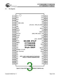
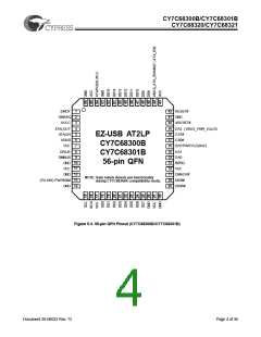
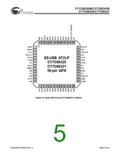
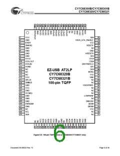
between the 68300B/01B and 68320/321 pinouts for the 56-
pin packages. For information on the CY7C68300A pinout,
please refer to the CY7C68300A data sheet that is found in the
“EZ-USB AT2” folder of the CY4615B reference design kit CD.
5.2
Pin Descriptions
The following table lists the pinouts for the 56-pin SSOP, 56-
pin QFN and 100-pin TQFP package options for the AT2LP.
Please refer to the Pin Diagrams in section 5.1 for differences
Table 5-1. AT2LP Pin Descriptions
Note: (Italics pin names denote pin functionality during CY7C68300A-compatibility mode)
56
56
100
Pin DefaultState
Type at Start-up
SSOP QFN TQFP
Pin Name
DD13
Pin Description
1
2
3
4
5
50
51
96
97
I/O[1]
I/O[1]
I/O[1]
GND
I/O
Hi-Z
Hi-Z
Hi-Z
ATA Data bit 13.
ATA Data bit 14.
ATA Data bit 15.
Ground.
DD14
52
98
DD15
53
54[3]
99
100[3]
GND
ATAPUEN
ATA pull-up voltage source for bus-powered applica-
tions (see section 5.3.10).
(NC)
Alternate Function: Input when the EEPROM config-
uration byte 8 has bit 7 set to one. The input value is
reported through EP1IN (byte 0, bit 2).
6
7
55
56
1
1
2
3
4
VCC
GND
PWR
GND
I[1]
VCC. Connect to 3.3V power source.
Ground.
8
IORDY
DMARQ
GND
Input
Input
ATA Control.
9
2
I[1]
ATA Control.
N/A
N/A
5
6
7
8
Ground.
10
3
9
AVCC
PWR
Analog VCC. Connect to VCC through the shortest path
possible.
11
12
13
4
5
6
10
11
12
XTALOUT
XTALIN
AGND
Xtal
Xtal
Xtal
Xtal
24-MHz Crystal Output (see section 5.3.3).
24-MHz Crystal Input (see section 5.3.3).
GND
Analog Ground. Connect to ground with as short a
path as possible.
N/A
N/A
13
14
15
NC
No Connect.
14
15
7
8
16
17
18
19
20
21
22
VCC
DPLUS
DMINUS
GND
PWR
I/O
VCC. Connect to 3.3V power source.
USB D+ Signal (see section 5.3.1).
USB D– Signal (see section 5.3.1).
Ground.
Hi-Z
Hi-Z
16
9
I/O
17
10
11
12
N/A
GND
PWR
GND
I
18
VCC
VCC. Connect to 3.3V power source.
Ground.
19
GND
N/A
SYSIRQ
Input
Active HIGH. USB interrupt request (see section
5.3.4). Tie to GND if functionality is not used.
N/A
20
N/A
23
24
25
26[3]
GND
GND
I/O
Ground.
13[3]
PWR500#[2]
(PU 10K)
Active LOW. VBUS power granted indicator used in
bus-powered designs (see section 5.3.11).
Alternate Function for 68320.
Reserved. Tie to GND.
21
14
27
GND (RESERVED)
Notes:
1. If byte 8, bit 4 of the EEPROM is set to ‘0’, the ATA interface pins are only active when VBUS_ATA_EN is asserted. See section 5.3.9.
2. A ‘#’ sign after the pin name indicates that it is active LOW.
3. The General Purpose inputs can be enabled on ATAPUEN, PWR500#, and DRVPWRVLD via EEPROM byte 8, bit 7 on CY7C68320/CY7C68321.
Document 38-08033 Rev. *D
Page 7 of 36

 CYPRESS [ CYPRESS ]