CY7C68300B/CY7C68301B
CY7C68320/CY7C68321
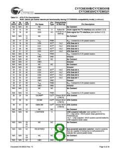
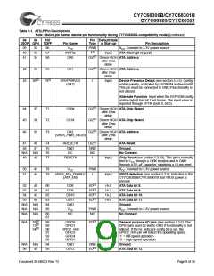
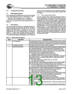
Table 5-1. AT2LP Pin Descriptions
Note: (Italics pin names denote pin functionality during CY7C68300A-compatibility mode) (continued)
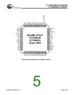
56
56
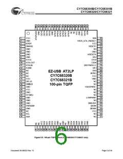
100
Pin DefaultState
Type at Start-up
SSOP QFN TQFP
Pin Name
VCC
Pin Description
VCC. Connect to 3.3V power source.
ATA Interrupt request.
39
40
41
32
33
34
66
67
68
PWR
INTRQ
DA0
I[1]
Input
O/Z[1] Driven HIGH ATA Address.
after 2 ms
delay
42
43
35
69
DA1
O/Z[1] Driven HIGH ATA Address.
after 2 ms
delay
36[3]
70[3]
DRVPWRVLD
I
Input
Device Presence Detect (see section 5.3.5). Config-
urable polarity, controlled by EEPROM address 0x08.
This pin must be connected to GND if functionality is
not utilized.
(DA2)
Alternate Function: Input when the EEPROM config-
uration byte 8 has bit 7 set to one. The input value is
reported through EP1IN (byte 0, bit 0).
44
45
46
37
38
39
71
72
73
CS0#
CS1#
O/Z[1] Driven HIGH ATA Chip Select.
after 2 ms
delay
O/Z[1] Driven HIGH ATA Chip Select.
after 2 ms
delay
O/Z[1] Driven HIGH ATA Address.
DA2
(VBUS_PWR_VALID)
after 2 ms
delay
47
48
40
41
74
75
76
77
ARESET#
GND
O/Z[1]
GND
NC
ATA Reset.
Ground.
N/A
49
N/A
42
NC
No Connect.
RESET#
I
Input
Input
Chip Reset (see section 5.3.13). This pin is normally
tied to VCC through a 100K resistor, and to GND
through a 0.1-µF capacitor, supplying a 10-ms reset.
50
51
43
44
78
79
VCC
PWR
I
VCC. Connect to 3.3V power source.
VBUS_ATA_ENABLE
VBUS detection (see section 5.3.9). Indicates to the
CY7C68300B/CY7C68301B that VBUS power is
present.
(ATA_EN)
52
53
45
46
80
81
82
83
84
85
DD8
DD9
DD10
DD11
GND
VCC
I/O[1]
I/O[1]
I/O[1]
I/O[1]
Hi-Z
Hi-Z
Hi-Z
Hi-Z
ATA Data bit 8.
ATA Data bit 9.
54
47
ATA Data bit 10.
ATA Data bit 11.
Ground.
55
48
N/A
N/A
N/A
N/A
N/A
N/A
PWR
NC
VCC. Connect to 3.3V power source.
No Connect.
86
87
NC
N/A
36[3]
13[3]
54[3]
88
89
90
91
92
93
GPIO0
GPIO1
GPIO2_nHS
GPIO3
I/O[3]
General purpose I/O pins (see section 5.3.6). The
GPIO pins must be tied to GND if functionality is not
utilized. If the hs_indicator config bit is set, the
GPIO2_nHS pin will reflect the operating speed:
‘1’ = full-speed operation.
GPIO4
GPIO5
‘0’ = high-speed operation.
N/A
56
N/A
49
94
95
GND
GND
I/O[1]
Ground.
DD12
Hi-Z
ATA Data bit 12.
Document 38-08033 Rev. *D
Page 9 of 36

 CYPRESS [ CYPRESS ]