X40430/X40431 – Preliminary Information
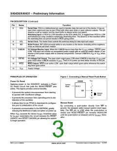
PIN DESCRIPTION (Continued)
Pin
Name
Function
8
SDA
Serial Data. SDA is a bidirectional pin used to transfer data into and out of the device. It has an
open drain output and may be wire ORed with other open drain or open collector outputs. This pin
requires a pull up resistor and the input buffer is always active (not gated).
Watchdog Input. A HIGH to LOW transition on the SDA (while SCL is toggled from HIGH to LOW
and followed by a stop condition) restarts the Watchdog timer. The absence of this transition within
the watchdog time out period results in WDO going active.
9
SCL
WP
Serial Clock. The Serial Clock controls the serial bus timing for data input and output.
10
Write Protect. WP HIGH prevents writes to any location in the device (including all the registers).
It has an internal pull down resistor.
11
V3MON
V3 Voltage Monitor Input. When the V3MON input is less than the V
voltage, V3FAIL goes
TRIP3
LOW. This input can monitor an unregulated power supply with an external resistor divider or can
monitor a third power supply with no external components. Connect V3MON to V or V
when
SS
CC
not used.
12
13
14
V3FAIL
WDO
V3 Voltage Fail Output. This open drain output goes LOW when V3MON is less than V
and
TRIP3
goes HIGH when V3MON exceeds V
. There is no power up reset delay circuitry on this pin.
TRIP3
WDO Output. WDO is an active LOW, open drain output which goes active whenever the watch-
dog timer goes active.
V
Supply Voltage
CC
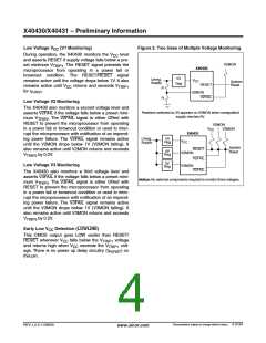
PRINCIPLES OF OPERATION
Power On Reset
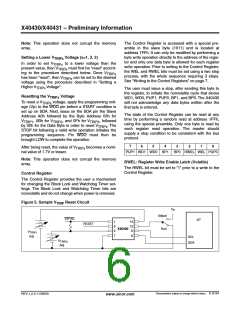
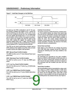
Figure 1. Connecting a Manual Reset Push-Button
V
CC
X40430
Applying power to the X40430/31 activates a Power
On Reset Circuit that pulls the RESET/RESET pins
active.This signal provides several benefits.
System
Reset
RESET
MR
– It prevents the system microprocessor from starting
to operate with insufficient voltage.
Manual
Reset
– It prevents the processor from operating prior to sta-
bilization of the oscillator.
Manual Reset
– It allows time for an FPGA to download its configura-
tion prior to initialization of the circuit.
By connecting a push-button directly from MR to
ground, the designer adds manual system reset capa-
bility. The MR pin is LOW while the push-button is
closed and RESET/RESET pin remains HIGH/LOW
until the push-button is released and for t
after.
– It prevents communication to the EEPROM, greatly
reducing the likelihood of data corruption on power up.
When V
exceeds the device V
threshold value
CC
TRIP1
there-
PURST
for t
(selectable) the circuit releases the RESET
PURST
(X40431) and RESET (X40430) pin allowing the system
to begin operation.
Characteristics subject to change without notice. 3 of 24
REV 1.2.3 11/28/00
www.xicor.com

 XICOR [ XICOR INC. ]