Electrical Characteristics T = 25°C unless otherwise noted
A
Symbol
Parameter
Test Conditions
Min
Typ
Max
Units
Off Characteristics
B
Drain to Source Breakdown Voltage
Zero Gate Voltage Drain Current
Gate to Source Leakage Current
I
= 250µA, V = 0V
200
-
-
-
-
-
V
VDSS
D
GS
V
V
V
= 200V, V = 0V
-
-
-
25
DS
DS
GS
GS
I
µA
nA
DSS
GSS
o
= 160V
20V
T
= 150
250
100
C
I
=
On Characteristics
V
r
Gate to Source Threshold Voltage
V
I
= V , I = 250µA
2
-
-
0.102
-
4
0.15
-
V
Ω
S
GS(TH)
GS
DS
D
Drain to Source On Resistance
Forward Transconductance
= 11A, V = 10V
GS
DS(ON)
D
g
V
= 50V, I = 11A (Note 2)
6.8
fs
DS
D
Dynamic Characteristics
C
C
C
Input Capacitance
-
-
-
2200
400
120
117
64
-
pF
pF
pF
nC
nC
nC
nC
nC
ISS
V
= 25V, V = 0V,
DS
GS
Output Capacitance
-
-
OSS
RSS
f = 1MHz
Reverse Transfer Capacitance
Total Gate Charge at 20V
Total Gate Charge at 10V
Threshold Gate Charge
Gate to Source Gate Charge
Gate to Drain “Miller” Charge
Q
Q
Q
Q
Q
V
V
V
= 0V to 20V
= 0V to 10V
= 0V to 2V
152
83
7
g(TOT)
g(10)
g(TH)
gs
GS
GS
GS
-
-
-
-
V
=100V
DD
= 22A
I
5
D
I = 1.0mA
g
9
-
24
-
gd
Switching Characteristics (V = 10V)
GS
t
t
t
t
t
t
Turn-On Time
Turn-On Delay Time
Rise Time
-
-
-
-
-
-
-
44
-
ns
ns
ns
ns
ns
ns
ON
10
19
23
5.5
-
d(ON)
-
r
V
V
= 100V, I = 11A
D
DD
GS
= 10V, R = 2.5Ω
Turn-Off Delay Time
Fall Time
GS
-
d(OFF)
-
f
Turn-Off Time
46
OFF
Drain-Source Diode Characteristics
V
t
Source to Drain Diode Voltage
Reverse Recovery Time
I
I
I
= 11A
-
-
-
-
-
-
1.3
251
V
SD
SD
SD
SD
= 11A, dI /dt = 100A/µs
ns
nC
rr
SD
Q
Reverse Recovered Charge
= 11A, dI /dt = 100A/µs
1394
RR
SD
Notes:
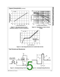
1: Starting T = 25°C, L = 4.2mH, I = 11A.
J
AS
2: Pulse width ≤ 400µs; duty cycle ≤ 2%.
©2002 Fairchild Semiconductor Corporation
Rev. B

 FAIRCHILD [ FAIRCHILD SEMICONDUCTOR ]