产品
最近搜索
热门搜索
发布采购
半导体可燃气体传感器是一种用于检测可燃气体浓度的传感器。它基于半导体材料的敏感性,通过测量传感元件的电学性质变化来判断目标气体的浓度。下面将...
日期:6小时前
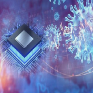
华为在AI领域的最新进展——Ascend 910B AI芯片的发布,标志着该公司在全球人工智能计算领域迈出了重要一步。Ascend 910B...
日期:6小时前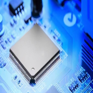
无源高压探头是一种用于电磁兼容(EMC)测试的设备,用于测量高压环境中电压信号的传感器,主要用于检测电子设备中存在的电磁干扰和辐射问题。它通...
日期:7小时前
随着科技的飞速发展,数据存储技术在现代社会中扮演着越来越重要的角色。无论是智能手机、平板电脑,还是数据中心,存储芯片都是核心组成部分。然而,...
日期:7小时前

中央水泵房是供水系统中的重要组成部分,负责供应稳定的水源。水位传感器作为中央水泵房的关键设备之一,用于监测水位并控制水泵的运行。然而,水位传...
日期:8小时前
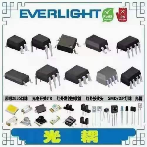
光隔离器和光耦合器是光电子学中的重要组件,广泛应用于各种电子和光学设备中。它们在隔离、保护和信号传输方面发挥着重要作用。本文将详细探讨光隔离...
日期:8小时前

专业IC领域供求交易平台:提供全面的IC Datasheet资料和资讯,Datasheet 1000万数据,IC品牌1000多家。